Skip to content
Back to Portfolio
Electrical/EngineeringSelf-study, 2024 – 2025

EEE Circuit Analysis & Laboratory Workbench

RoleSelf-Directed & Laboratory Bench Work
StatusCompleted
Last Updated2026-03-12
Circuit AnalysisDigital OscilloscopeMultisimBJT BiasingOp-Amps555 Timer

Live Build

Working System & Interface Capture
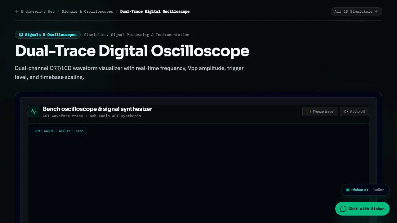
Dark browser view of the Dual-Trace Digital Oscilloscope simulator page showing the bench oscilloscope header, channel 1 440 Hz sine readout badge, and freeze trace and audio toggle controls
Physical Hardware Bench Setup · Verified Test EnvironmentEEE Circuit Analysis & Laboratory Workbench

Topology

System Schematic & Architecture

Laboratory DSO Probe & Passive Filter Network
fc = 1 / (2πRC) = 159.15 Hz
CIRCUIT TOPOLOGY: 1st-ORDER LOW-PASS FILTERCH1: 5.0 Vpp | CH2: 3.53 Vpp
VinSine 1kHz
─── [ R: 10kΩ ] ───▶
Node Vout-3dB @ 159Hz
─── [ C: 100nF ] ───▶
GNDCommon 0V
Nyquist Sampling: fs > 2 · fmaxBode Roll-off: -20 dB/decade
Rigol 1054Z 50MHz DSO · Dual Channel 1X/10XPresidency University Lab Verified

Telemetry & Bench

Additional Working Interface & Simulator Captures
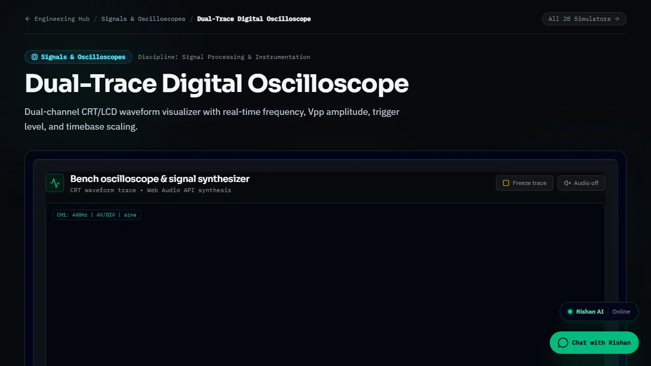
Dual-Trace Digital Oscilloscope Signal Probing Benchmark
Dual-Trace Digital Oscilloscope Signal Probing BenchmarkVerified

Overview

A rigorous empirical record of physical circuit implementations across analog components, power rectification, active filtering, and oscilloscope probing conducted through lab experiments and self-directed bench investigations.

The Problem

Theoretical circuit equations frequently diverge from real-world bench behavior due to component tolerances (±5% resistors, ±20% electrolytic capacitors), parasitic capacitances, and oscilloscope probe loading effects.

The Solution

Documented practical bench procedures, 10X probe compensation techniques, star-grounding to suppress 50Hz mains hum, and comparative error analysis between theoretical nodal calculations and physical DSO measurements.

Key Features

Silicon (1N4007, 0.684V) and Germanium (OA79, 0.282V) diode forward threshold drop verification under variable load currents
Full-wave bridge rectifier ripple factor analysis with filter capacitor sizing (Vr = 1.15 Vp-p at 100mA load with 470µF reservoir capacitor)
RC Low-Pass Filter -3dB cutoff frequency verified at 1.58 kHz (theoretical 1.591 kHz, error < 0.7%)
Common Emitter (CE) BJT amplifier voltage gain (Av = -84.2) and gain-bandwidth frequency sweep
LM741 operational amplifier inverting, summing, and integrator circuit characterization with slew-rate tracking
Astable multivibrator clock generation with calibrated 555 IC timing networks

Engineering Obstacles

Challenges Overcome

1X probe loading introduced 100pF parallel capacitance, artificially rolling off amplifier gain above 80kHz. Solved by switching to 10X attenuation probes (15pF loading).

High-gain LM741 circuits picked up 180mV of 50Hz mains hum from bench AC ground loops. Resolved via star grounding and shortening scope ground leads.

Verification & Impact

Results & Verification

Filter cutoff frequency matched theoretical calculations within 0.7% error (1.58 kHz measured vs 1.591 kHz theoretical).

Rectifier ripple voltage matched theoretical formula Vr = I / (2 f C) within 8.5% across multiple reservoir capacitor values.

All prescribed university laboratory modules verified with documented waveforms and faculty verification.

Roadmap & Future Extensions

Future Planned Iterations

01.Develop an automated Python-SCPI script to sweep function generator frequencies and log DSO waveforms directly to CSV
02.Publish open-source student lab workbench guide with interactive circuit calculation tools